![]()
![]()
Hello and Welcome to the SECOND release of the new HARDWARE LAB department where I'm going to review popular hardware components, accessories etc.
Today's topic is NVIDIA GeForce FX 5900 Graphics Adapter.
Intro
"The king is dead - long live for the new king!" I think this phrase is the most suitable for the beginning. Why ? You will know it in the end...
First, I want to sympathize with the ones who have already spent 500$ or so when buying a GeForce FX 5800 (NV30) graphics adapter. NVIDIA has deceived its customers again.
The hardware world hadn't come down after the release of NV30 when the new NV35 was officially announced ! It was just after a month from the NV30 release date. There is also one thing that should be admitted - the recent NVIDIA press-conference where their president promised the release of NV35 and called NV30 a mistake or some kind of an unlucky release ! What about the customers that bought NV30 ? NV30 -> NV35 upgrade is not free of course. That's where the NV30 purchasers lost...
As well as NV30, NV35 is not just one video card, it's a new series:
![]() GeForce FX 5900 Ultra � 450
MHz core, 256 MB 425 MHz (DDR 850) memory, 256 bit local memory bus ($499);
GeForce FX 5900 Ultra � 450
MHz core, 256 MB 425 MHz (DDR 850) memory, 256 bit local memory bus ($499);
![]() GeForce FX 5900 � 450 MHz core, 128 MB 425
MHz (DDR 850) memory, 256 bit local memory bus ($399).
GeForce FX 5900 � 450 MHz core, 128 MB 425
MHz (DDR 850) memory, 256 bit local memory bus ($399).
Some specifications of course will be changing but at this moment, the fastest NVIDIA Graphics Adapter - GeForce FX 5900 Ultra (codename: NV35) was tested. The change of second number (0 to 5) in NV30 - NV35 chips could mean the minimum of changes in the new adapter or just an overclocking of it. But NV35 frequencies are even lower but.. 256-bit memory bus is provided....
There's one thing that is surely defined - NV35 is NOT a CONTINUATION of NV30 (like NVIDIA did with GeForce3-GeForce4), it's a REPLACEMENT of NV30.
Technical Characteristics
![]() 0,13 Micron
Technology Process, copper catenation.
0,13 Micron
Technology Process, copper catenation.
![]() 135 million of transistors
135 million of transistors
![]() 3 geometric processors (exceeding
specifications of DX9 VS 2.0)
3 geometric processors (exceeding
specifications of DX9 VS 2.0)
![]() 4 imporved conveyor pixel processors.
Their functionality exceeds DirectX9 PS 2.0 specifications noticeably,
two times more powerful than shaders in NV30 and operations, that use floating
point (GLOPS), are performed with full 128 bit accuracy.
4 imporved conveyor pixel processors.
Their functionality exceeds DirectX9 PS 2.0 specifications noticeably,
two times more powerful than shaders in NV30 and operations, that use floating
point (GLOPS), are performed with full 128 bit accuracy.
![]() AGP 3.0 (8�) System Interface
AGP 3.0 (8�) System Interface
![]() 256-bit interface of DDR1(!) local memory
256-bit interface of DDR1(!) local memory
![]() Intellisample HCT (High Compression Technology)
is an improved Intellisample technology provided in NV30 - saving of local
memory's capacity.
Intellisample HCT (High Compression Technology)
is an improved Intellisample technology provided in NV30 - saving of local
memory's capacity.
![]() Other optimizations of caching, compression
and early cutting off of invisible surfaces (Early HSR, Early z Cull)
Other optimizations of caching, compression
and early cutting off of invisible surfaces (Early HSR, Early z Cull)
![]() UltraShadow Technology - increases the
speed of stencil shadows formation.
UltraShadow Technology - increases the
speed of stencil shadows formation.
![]() Support of accurate integer formats (10/16
bit for the multiplier) and accurate floating formats (16 and 32 bit for the
multiplier) for frames and textures buffering.
Support of accurate integer formats (10/16
bit for the multiplier) and accurate floating formats (16 and 32 bit for the
multiplier) for frames and textures buffering.
![]() End-to-end accuracy of all operations �
32-bit floating arithmetics
(support of so called 128-bit light depth)
End-to-end accuracy of all operations �
32-bit floating arithmetics
(support of so called 128-bit light depth)
![]() The new algorithm for optimized anisotropic
filtering, if activated, decreases the loss of performance quality not lowering
much of the total quality.
The new algorithm for optimized anisotropic
filtering, if activated, decreases the loss of performance quality not lowering
much of the total quality.
![]() Bilinear-to-8x Anisotropy quality
Bilinear-to-8x Anisotropy quality
![]() Support of "hybrid" modes �� � 8� and 6xS
Support of "hybrid" modes �� � 8� and 6xS
![]() Frame buffer compression allows the
decrease of productivity loss when activating FSAA mode.
Frame buffer compression allows the
decrease of productivity loss when activating FSAA mode.
![]() Two built-in RAMDACs 400
Two built-in RAMDACs 400
![]() �uilt-in interface for external TV-Out
chip.
�uilt-in interface for external TV-Out
chip.
![]() Built-in-the-chip 3 TDMS-channels for
external front-end DVI chips
Built-in-the-chip 3 TDMS-channels for
external front-end DVI chips
Now more detailed:
![]() Chip with
135 million transistors: the quantity of transistors was increased not
by much compared with NV30. This means that changes and modifications of
NV35 are not global and are just upgrades/updates.
Chip with
135 million transistors: the quantity of transistors was increased not
by much compared with NV30. This means that changes and modifications of
NV35 are not global and are just upgrades/updates.
![]() 256-bit local memory interface:
surely the most expected innovation in NV35. After the release of NV30,
graphics enthusiasts couldn't even imagine NV35 without this option when
predicting this chip's characteristics.
256-bit local memory interface:
surely the most expected innovation in NV35. After the release of NV30,
graphics enthusiasts couldn't even imagine NV35 without this option when
predicting this chip's characteristics.
![]() 4 improved conveyor pixel
processors: Increase to 8 processors was expected but NVIDIA decided
to leave 4.
Each pixel processor is designed with 2 textures filtering blocks, 2
mixed integral and ALU (floating point operations) blocks and 1 ALU block,
that deals only with floating point operations. So 3 floating point
operations per clock. This configuration allows the fulfillment of 12
pixel operations per clock.
But at the moment this only works for OpenGL; in Direct3D still the same
- 1 floating-point operation per clock (although this is promised to be
fixed). As admitted in the press-release, the new NV35 surpasses NV30 in
power of processors by 2 in filling pixel shaders of
DirectX9 PS 2.0 with 128-bit calculations' accuracy.
4 improved conveyor pixel
processors: Increase to 8 processors was expected but NVIDIA decided
to leave 4.
Each pixel processor is designed with 2 textures filtering blocks, 2
mixed integral and ALU (floating point operations) blocks and 1 ALU block,
that deals only with floating point operations. So 3 floating point
operations per clock. This configuration allows the fulfillment of 12
pixel operations per clock.
But at the moment this only works for OpenGL; in Direct3D still the same
- 1 floating-point operation per clock (although this is promised to be
fixed). As admitted in the press-release, the new NV35 surpasses NV30 in
power of processors by 2 in filling pixel shaders of
DirectX9 PS 2.0 with 128-bit calculations' accuracy.
![]() Intellisample HCT :
technology of saving of local memory's capacity - compression without
frame buffer losses, including a color information as well as the Z-Buffer
information. Probable compression coefficient is to 4:1. The
Intellisample technology was used in NV30 as well but in NV35 the
probability of an effective compression is higher due to Intellisample
optimization. Intellisample HCT also includes the following technologies
of working with local memory : local memory controller with multiplexer,
texture caches,
early cutting off of invisible pixels (z-culling), early clearance of
depth buffer (fast z-clear). All these optimizations allow to reduce a
performance decrease of the video chip when activating an FSAA mode.
Intellisample HCT :
technology of saving of local memory's capacity - compression without
frame buffer losses, including a color information as well as the Z-Buffer
information. Probable compression coefficient is to 4:1. The
Intellisample technology was used in NV30 as well but in NV35 the
probability of an effective compression is higher due to Intellisample
optimization. Intellisample HCT also includes the following technologies
of working with local memory : local memory controller with multiplexer,
texture caches,
early cutting off of invisible pixels (z-culling), early clearance of
depth buffer (fast z-clear). All these optimizations allow to reduce a
performance decrease of the video chip when activating an FSAA mode.
![]() UltraShadow Technology: this
technology allows to increase the speed of visualization of shadows when
using stencil buffer shadows, technology used in DOOM III game. As a part
of UltraShadow technology, the opportunity of doubling the fillrate thus
filling 8 pixels per clock if only Z-buffer or stencil buffer is filled
(compare it with 4 pixels per clock in the usual rendering) in NV30/NV35
is also declared. The second, most interesting part is that there is a
possibility of assigning range of depth in the frame, where the object can
discard the shadow. The following block-scheme illustrates the technology:
UltraShadow Technology: this
technology allows to increase the speed of visualization of shadows when
using stencil buffer shadows, technology used in DOOM III game. As a part
of UltraShadow technology, the opportunity of doubling the fillrate thus
filling 8 pixels per clock if only Z-buffer or stencil buffer is filled
(compare it with 4 pixels per clock in the usual rendering) in NV30/NV35
is also declared. The second, most interesting part is that there is a
possibility of assigning range of depth in the frame, where the object can
discard the shadow. The following block-scheme illustrates the technology:
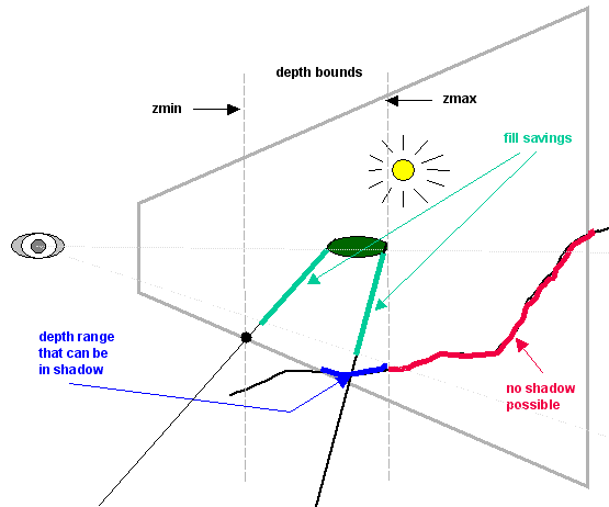
If during the shadows processing pixel's depth value, stored in the depth buffer (Z-buffer), misses the assigned range; stencil buffer for the pixel is not updated. Thus the saving of a pretty high percentage of filling rate (or just fillrate) becomes available. It seems that there's a modified block, that is charged in the early culling of invisible surfaces (early z-cull) in chip designed for the achievement of this function and that now collates the value stored in the Z-buffer not only with the current value ( it's intercalary reasoning from the triangle coordinates) but with two additional values. As a result, benefits in comparison with other chips with the same quantity of conveyors will be twice bigger as a last resort (8 Z-buffer values in comparison with 4 color values) and 4 times bigger (taking into consideration that an early z-cull can discard to 16 pixels per clock) even without taking into consideration the decrease of data capacity recorded back in the local memory.
However, the technology has the following limits:
![]() UltraShadow
Technology will be available only in OpenGL applications by applying
UltraShadow
Technology will be available only in OpenGL applications by applying the "NV_depth_bounds_test"
extensions
![]() NVIDIA is waiting for the taking out of the
patent for UltraShadow.
NVIDIA is waiting for the taking out of the
patent for UltraShadow.
![]() The technology cannot be activated by
applying a few code lines - programmers have to analyze the represented
scene and assign the range, where the shadows processing is possible,
effectively.
The technology cannot be activated by
applying a few code lines - programmers have to analyze the represented
scene and assign the range, where the shadows processing is possible,
effectively.
![]() At this moment the technology is announced
only for NV35, the extension in current drivers is available only for NV35. It's
still a question if this extension will be available for NV3x chips, although
there is a positive signal as the extension
At this moment the technology is announced
only for NV35, the extension in current drivers is available only for NV35. It's
still a question if this extension will be available for NV3x chips, although
there is a positive signal as the extension
"NV_depth_bounds_test" is available in the NV30 emulation
mode in
"Buzz/emulated" option of the OpenGL driver, released in early August,
2002.
The Chip
| DDR memory cards by Hynix of the HY5DU283222-AF22 trademark, BGA form-factor. The maximum memory frequency rate � 450 (900) MHz, fetch time � 2.2 ns. The following values are set by default: 425 (850) MHz of memory frequency, 450 MHz of chip frequency. |
 |
It's possible to see that the quantity of microchips for providing 256 MB of local memory is twice bigger than usual. The memory works on the two-way banking system that gives an increase of speed of working with it.
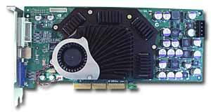
| NVIDIA GeForce FX 5900 Ultra 256MB | |
|---|---|
 |
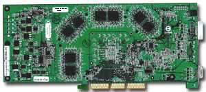 |
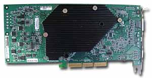
| NVIDIA GeForce FX 5800 Ultra 128MB | |
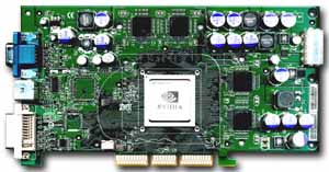 |
 |
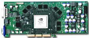
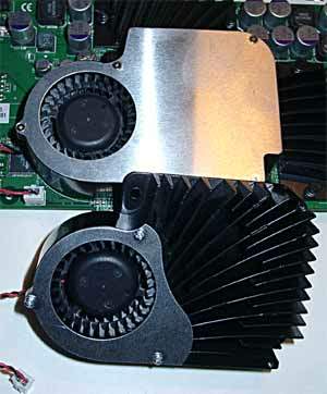
One of the most fascinating point is cooling. Many expected to see something different from an FX Flow cooling system used for NV30 and "as noisy as a helicopter".
|
The cooling system consists of two coolers - for
the memory and the processor. The central cooler looks like the one
used for Quadro FX and GeForce FX 5800 (not Ultra)
but with "cut off" cover on the radiator,
that reduces the noise. The cooler works in the same way: spinning on
small turns normally and accelerating when the temperature of the chip
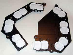
becomes critical. The system of memory cooling consists of two massive aluminium black radiators. The heat is transported through the special thermo elements, glued with the radiators. They also guarantee the full clamping to the memory microchips. At all, the bracing of the whole system is very well thought-out, no more plastic clips, everything's clamped using bolts and springs. |
 |
 | |
 |
Note, that heating of the chip is MUCH smaller than the one of NV30. The total heating of radiators is slightly bigger than the pain barrier of human.
Finishing with the chip review, I would like to
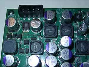
add the the whole "back" of the chip is dedicated to the power supply.
There's a socket for connecting the chip with an external source of power
supply (for example, Uninterruptible Power Supply - UPS)
The technical review of NV35
is now finished... BUT YOU CAN GO ON READING ABOUT IT IN THE OTHER DEPARTMENTS:
SOFTWARE EXCLUSIVE DEPARTMENT
------
NVIDIA GeForce FX 5900 (NV35) Drivers Setup
HARDWARE BENCHMARKS ------ NVIDIA GeForce FX 5900 (NV35) Benchmark Testing
P o s t e d b y M @ j e $ t | c
O n 1 6 . 0 5 . 2 0 0 3
17:00 GMT